Research and development in the Second Stage
Development of Observation and Fabrication Support System for Ultra Fine Object
Innovative nanotechnologies for detection, machining, measurement, and production of nanosized objects are developed for medical, agricultural, biological science, chemistry, and industry.3-1 Nano Imaging Technique for Clarifying Biofunction
 Project Leader:
Professor Yoshimasa Kawata, Faculty of Engineering, Shizuoka University
URL http://optsci.eng.shizuoka.ac.jp
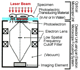
New opt-electronic microscope having high resolution of smaller than 10 nanometers is under development for imaging of living biological specimens. It is built by combining the best features of optical-microscope and electromicroscopes to take the image of a biological specimen in living condition and with very high magnification provided by electron microscopes.
3-2 Nano Machining System Coupled with Optical Manipulator
 Project Leader:
Associate Professor Futoshi Iwata, Faculty of Engineering, Shizuoka University
URL http://tf2a14.eng.shizuoka.ac.jp/
Scanning probe microscopes (SPM) and atomic force microscopes (AFM) have a function as a knife in nano-scale machining. They can process nano-scale machining. A laser manipulator has a function as tweezers for nano-scale objects. They can pick and handle ultra small objects.
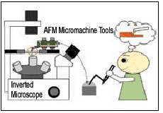 The developed device is a new integrated machine of new scanning probe microscope systems with machining and manipulator functions. The device is used for an inspection and processing machine for nano-sized objects. The great possibility of using the device is expected for many applications in industry and bio-fields.
3-3 Detection and 3D Imaging of Ultra Small Object using Superconducting Magnetic Sensor
 Project Leader:
Professor Saburo Tanaka, Department of Ecological Engineering, Toyohashi University of Technology,
URL http://www.eco.tut.ac.jp/%7Etanakas/tanakas.html
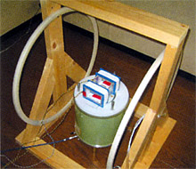
New device is currently under development to detect extremely tiny metal substances that is not detected by conventional technology. The device is the SQUID (super-conducting quantum interference device) having extremely high sensitivity of 1 billionth of the magnetism of earth.
3-4 Nanostructure Embedded Phosphor Particles and Ultra-High-Output UV Source
 Project Leader:
Professor Kazuhiko Hara, Research Institute of Electronics, Shizuoka University
URL http://ny7084.rie.shizuoka.ac.jp/active-display/
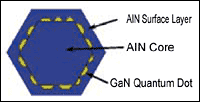
New flat panels of ultraviolet high-output source are currently under development, using electron beam excitation of UV phosphor particle of sub-micrometer diameter. Each particle has numerous atomic sized dots such as GaN (gallium nitride) inlaid in the particle.
 This ultraviolet light source will serve as a safe substitute for the currently used mercury lamps needed in many applications in industrial and medical treatment fields, etc.