Research and development in the Second StageResearch and development in the Second Stage
Development of High Functional Imaging Devices and Intellectual Information Process
Along with imaging, measuring, and communication devices for traffic handling, industrial,medical, and information processing, work is also underway on developing device applications as support technology to build a safe, secure, and comfortable world around us.1-1 Highly Sensitive Uncooled CMOS Image Sensor
 Project Leader:
Professor Shoji Kawahito, Research Institute of Electronics, Shizuoka Universityö
URL http://www.idl.rie.shizuoka.ac.jp/
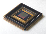
A super-low brightness image-capturing CMOS image sensor using noise-reduction, wide dynamic range (wide DR), and signal processing technology is under development as a high-sensitive light detector capable of capturing images over a wide brightness range even down to a single electron at room temperatures.
 Highly Functional CMOS Image Sensor
 |
The sensor is for a compact high-sensitivity wide DR camera needing no cooler device. It offers great possibilities in a wide range of applications such as bioimaging and scientific measuring camera for capturing ultra-weak light, night-vision cameras mounted in vehicles for finding pedestrians under the glow of oncoming vehicle headlights, and security cameras used for night-time surveillance of poorly illuminated areas, etc.
1-2 Image Sensor for Optical Information Communication
Project Leader:
Professor Shoji Kawahito, Research Institute of Electronics, Shizuoka University
Professor Shoji Kawahito, Research Institute of Electronics, Shizuoka University
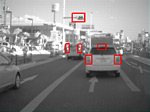
The sensor has new function to trace the light and communicate with the light of traffic signals or taillights. The sensor also shows great potential for use in short distance communication systems besides contributing to safe vehicle driving.
1-3 Development and Application of Time Correlation Image Sensor
 Project Leader:
Professor Shoji Kawahito, Research Institute of Electronics, Shizuoka University
Professor Shigeru Ando, Graduate School of Information Science and Technology, The University of Tokyo
URL http://www.alab.t.u-tokyo.ac.jp/~ando/index-j.html
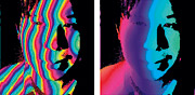
The time correlation image sensor was conceived by Prof. Ando as a sensor for irradiating a moving light pattern onto an object to acquire the image intensity signal distribution of the light the same as for an ordinary image, while also acquiring its time-correlated information. To allow high-speed sensor operation, Prof. Kawahito developed an entirely new timecorrelated image sensor that utilizes high-speed charge transfer technology.
1-4 Intelligent Image Sensor using Ferroelectric Thin Film on Epitaxial Oxide Layer for IR or Ultrasonic Waves
 Project Leader:
Professor Makoto Ishida, Department of Electrical and Electronic Engineering, Toyohashi University of Technology
URL http://icg.dev.eee.tut.ac.jp/index_j.html
Imaging devices that integrate ferroelectric thin films sensors and silicon integrated circuits are under development for sending and receiving infrared and ultrasonic waves with far greater sensitivity than was possible up till now. These sensors are fabricated by epitaxially developing a strong ferroelectric material with a polarized crystal orientation enclosing an oxidized film (epitaxial alumina film) on a silicon substrate.
1-5 Single-Electron Device and Information Compression Circuit with Single-Photon Sensitivity
 Project Leader:
Professor Hiroshi Inokawa, Research Institute of Electronics, Shizuoka University
URL http://www.rie.shizuoka.ac.jp/~nanosys/
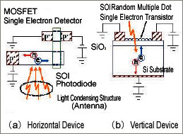
Single electron devices are highly sensitive electrical charge detectors and handles minimum electrical charges. New type photon detectors (Fig. (a) or Fig. (b)) capable of directly sensing single electron emitted by photons. The detector including low-power data compression circuits using single-electron transfer does not need any electron multipliers that usually cause noise and signal jitter. It is made using SOI (siliconon- insulation) technology for higher sensitivity, operating speed and temperature.
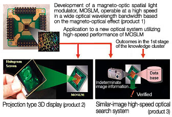
1-6 Wide-wavelength-band Super-high-speed MOSLM and Application to Optical IT System
 Project Leader:
Professor Mitsuteru Inoue, Department of Electrical and Electronic Engineering, Toyohashi University of Technology
URL http://www.maglab.eee.tut.ac.jp/
Current development work includes a magneto-optic spatial light modulator or MOSLM capable of high-speed operation over a wide optical wavelength band, and a highreality projection type 3D display that combines the MOSLM with holographic screen technology. The 3D display projects directional images that can be seen from wherever the viewer is watching.